Curriculum
Science Grade XII Physics
Science Grade XII Physics
0/14-
Chapter 1: Electric Charges and Fields
 Preview
 -
Chapter 2: Electrostatic Potential and Capacitance
Preview
-
Chapter 3: Current Electricity
Preview
-
Chapter 4: Moving Charges and Magnetism
Preview
-
Chapter 5: Magnetism and Matter
Preview
-
Chapter 6: Electromagnetic Induction
Preview
-
Chapter 7: Alternating Current
Preview
-
Chapter 8: Electromagnetic Waves
Preview
-
Chapter 9: Ray Optics and Optical Instruments
Preview
-
Chapter 10: Wave Optics
Preview
-
Chapter 11: Dual Nature of Radiation and Matter
Preview
-
Chapter 12: Atoms
Preview
-
Chapter 13: Nuclei
Preview
-
Chapter 14: Semiconductor Electronics
Preview
Chapter 14: Semiconductor Electronics
|
Grade 12 Science | Chapter 14 Semiconductor ElectronicsSemiconductors power modern electronics. This chapter develops energy bands, doping, the p-n junction and the diode as a rectifier, and the basic logic gates.
|
|
Contents
|
1. Introduction: Semiconductors |
Modern electronics, from phones to computers, is built on semiconductors, materials such as silicon whose ability to conduct lies between that of conductors and insulators. By controlling this conduction, we can build the tiny switches and components that make up every circuit. This chapter follows how semiconductors work and how they form the diode and the logic gates at the heart of electronics.
|
Core idea A semiconductor conducts in between a conductor and an insulator. Doping makes n-type and p-type material, and a p-n junction forms a diode that lets current flow one way.
|
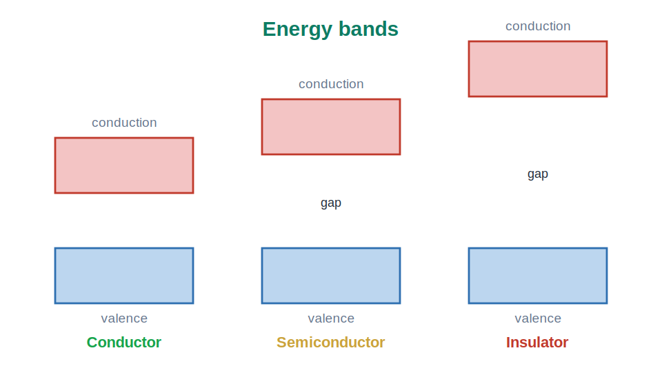
2. Energy Bands |
In a solid, the electron energies group into bands: a filled valence band and an empty conduction band, with an energy gap between them. In a conductor the bands overlap, so electrons move freely. In an insulator the gap is large, so few electrons can cross. In a semiconductor the gap is small, so a little energy lets some electrons jump and conduct.
|
Diagram 1 – Energy Bands
Fig 1. Conductors have overlapping bands, insulators a large gap, and semiconductors a small gap. |
3. Doping: n-type and p-type |
Pure silicon barely conducts, so we add tiny amounts of other elements, a process called doping, to control it. Adding an element with spare electrons gives n-type material, which conducts using extra free electrons. Adding an element short of electrons gives p-type material, which conducts using holes, the gaps where electrons are missing. Both kinds conduct far better than pure silicon.
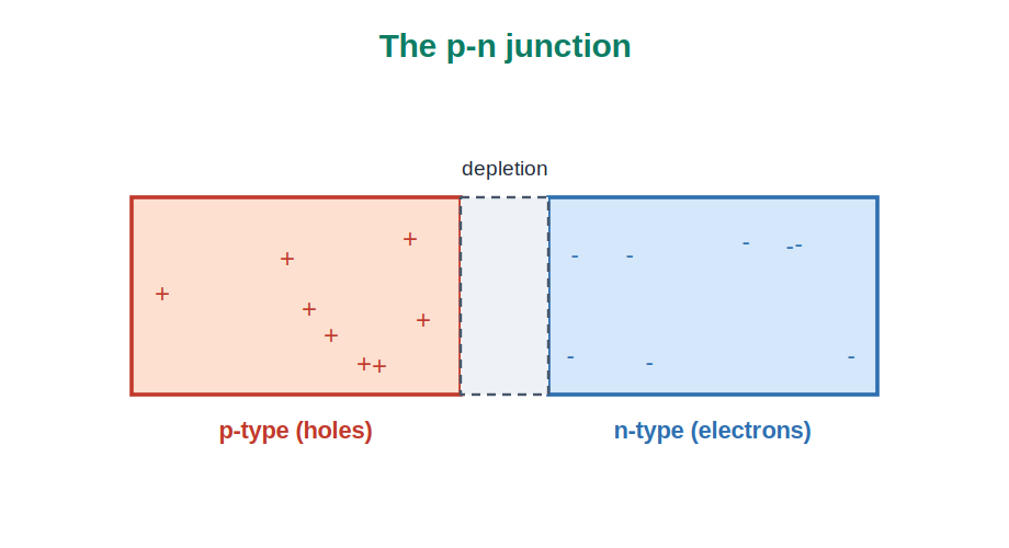
4. The p-n Junction |
Joining a piece of p-type to a piece of n-type forms a p-n junction, the basic building block of electronics. Where they meet, some electrons and holes combine, leaving a thin region with no free charges called the depletion region. This region sets up a barrier that allows current to pass easily in one direction but not the other, which is the key to the diode.
|
Diagram 2 – The p-n Junction
Fig 2. At a p-n junction a depletion region forms between the p-type and n-type material. |
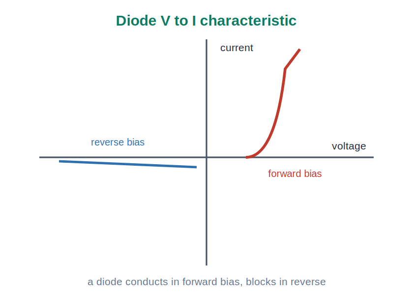
5. The Diode and Rectification |
A p-n junction used as a component is a diode. In forward bias, with the right voltage direction, it conducts; in reverse bias it blocks the current. Because it lets current flow only one way, a diode can turn alternating current into one directional current, a process called rectification. This is how the adapters that charge our devices convert mains AC into the DC the device needs.
|
Diagram 3 – Diode V to I Characteristic
Fig 3. A diode conducts in forward bias and blocks current in reverse bias. |
6. Logic Gates |
Semiconductors also build logic gates, the tiny circuits that carry out the logic of computers. Each gate takes inputs that are either on or off, written 1 or 0, and gives an output by a fixed rule. An AND gate outputs 1 only if all inputs are 1; an OR gate outputs 1 if any input is 1; a NOT gate reverses its input. From these simple gates, every digital circuit is built.
7. Key Reasoning (Principles) |
|
Principle 1: The band gap sets the conduction Overlapping bands make a conductor, a large gap an insulator, and a small gap a semiconductor that conducts with a little energy. |
|
Principle 2: Doping controls the charge carriers Adding spare electrons gives n-type material and creating holes gives p-type, so doping sets how a semiconductor conducts. |
|
Principle 3: A junction conducts one way The depletion region of a p-n junction lets current pass in forward bias but blocks it in reverse, which makes the diode a one way valve. |
8. Worked Examples |
| Example 1 |
|
Q: What is a semiconductor? ▶ Show SolutionA material that conducts between a conductor and an insulator. Answer: Conducts between conductor and insulator. |
| Example 2 |
|
Q: What decides whether a material conducts? ▶ Show SolutionThe size of the energy gap between the bands. Answer: The band gap. |
| Example 3 |
|
Q: What kind of gap does a semiconductor have? ▶ Show SolutionA small gap. Answer: A small gap. |
| Example 4 |
|
Q: What is doping? ▶ Show SolutionAdding tiny amounts of other elements to control conduction. Answer: Adding impurities to control conduction. |
| Example 5 |
|
Q: What carries the current in n-type material? ▶ Show SolutionExtra free electrons. Answer: Free electrons. |
| Example 6 |
|
Q: What carries the current in p-type material? ▶ Show SolutionHoles, the gaps where electrons are missing. Answer: Holes. |
| Example 7 |
|
Q: What forms at a p-n junction? ▶ Show SolutionA depletion region with no free charges. Answer: A depletion region. |
| Example 8 |
|
Q: When does a diode conduct? ▶ Show SolutionIn forward bias. Answer: In forward bias. |
| Example 9 |
|
Q: What is rectification? ▶ Show SolutionTurning alternating current into one directional current. Answer: Turning AC into DC. |
| Example 10 |
|
Q: What does an AND gate output? ▶ Show Solution1 only if all its inputs are 1. Answer: 1 only if all inputs are 1. |
9. Practice Sets A to D |
| Set A – Multiple Choice (Basic) |
|
1. A semiconductor conducts: (a) like a metal (b) between conductor and insulator (c) never (d) like an insulator only 2. An insulator has a band gap that is: (a) zero (b) small (c) large (d) negative 3. n-type material conducts using: (a) holes (b) electrons (c) protons (d) photons 4. A diode conducts in: (a) reverse bias (b) forward bias (c) both (d) neither 5. An OR gate outputs 1 if: (a) all inputs are 1 (b) any input is 1 (c) no input is 1 (d) inputs are equal ▶ Reveal Answers1. (b) between conductor and insulator. 2. (c) large. 3. (b) electrons. 4. (b) forward bias. 5. (b) any input is 1. |
| Set B – Short Answer (Understanding) |
|
1. Explain how the band gap decides conduction. 2. What is doping, and what are n-type and p-type? 3. What is the depletion region? 4. How does a diode behave in forward and reverse bias? 5. State what AND, OR and NOT gates do. ▶ Reveal Answers1. Overlapping bands give a conductor, a large gap an insulator, and a small gap a semiconductor. 2. Adding impurities to control conduction; n-type conducts by extra electrons, p-type by holes. 3. A thin region at a p-n junction with no free charges, where electrons and holes have combined. 4. It conducts in forward bias and blocks current in reverse bias. 5. AND outputs 1 only if all inputs are 1; OR outputs 1 if any input is 1; NOT reverses its input. |
| Set C – Application and Reasoning |
|
1. Why does a small band gap make a semiconductor? 2. Why does doping increase conduction? 3. Why does a diode allow current only one way? 4. Why is a diode used to make a charger? 5. Why are logic gates the basis of computers? ▶ Reveal Answers1. Because only a little energy is needed for electrons to cross into the conduction band and conduct. 2. Because it adds free electrons or holes that carry current far more than pure silicon. 3. Because the depletion region passes current in forward bias but blocks it in reverse. 4. Because it rectifies the mains alternating current into the one directional current the device needs. 5. Because they carry out logic on on or off signals, and combining them builds every digital circuit. |
| Set D – Higher Order (Challenge) |
|
1. Explain why a semiconductor conducts better when warmed, unlike a metal. 2. Explain how n-type and p-type differ in their charge carriers. 3. Explain how the depletion region acts as a one way valve. 4. Explain how a diode converts AC to DC. 5. Explain how simple gates can build a complex computer. ▶ Reveal Answers1. Because warming gives more electrons the energy to cross the small gap into the conduction band, so conduction rises, while in a metal heat hinders the electrons. 2. n-type carries current with extra free electrons, while p-type carries it with holes, the gaps left where electrons are missing. 3. Its barrier is lowered in forward bias so current flows, but raised in reverse bias so current is blocked, passing current one way only. 4. By conducting only during the half of the AC cycle that forward biases it, so the output flows in just one direction. 5. By combining AND, OR and NOT gates in vast numbers, every arithmetic and logical operation a computer performs can be built up. |
|
Chapter Summary
|
|||||||||||||||||||||||||||||||
| 8-Point Exam Quick-Check | ||||||||||||||||||||||||||||||||
|
||||||||||||||||||||||||||||||||
|
School Revise Virtual Lab Explore these ideas with interactive simulations and visual tools.
|
|
Class 12 Physics Chapter 14: Semiconductor Electronics, Complete Notes and Practice This revision guide follows the current NCERT Class 12 Physics syllabus and develops semiconductor electronics, covering energy bands in conductors, semiconductors and insulators, doping to make n-type and p-type material, the p-n junction and its depletion region, the diode and rectification, and the basic logic gates, with three diagrams, ten worked examples and graded practice. Visit SchoolRevise.com to revise, practise and excel. |